Technology Review - EMI shielding
Importance of understanding electromagnetic interference and the related industries
Electromagnetic wave is a form of energy that occurs due to the use of electricity, which has a broad range of frequency. Notably, studies have shown that lengthened exposure to frequency below 500KHz can harmful impacts on human body such as change in body temperature, reduction in number of sperms, and menstrual irregularity. Electromagnetic wave is accumulated in human body as a form of energy, producing harmful effects by reducing biorhythms. Recently, the rapid distribution of digital devices such as PC and cell phones are leading to a flood of electromagnetic waves throughout workplaces and households. Harms of such electromagnetic waves include computer malfunction, fire accidents in factories, and harmful effects on human body. Consequently, the technology for electromagnetic interference on various electrical and electronic products is rising as a key technological area in the electronics industry.
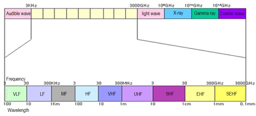
[Figure 1. Classification of electromagnetic waves by frequency]
Age of IoT and electromagnetic pollution
According to “Comprehensive measures on protecting human body from electromagnetic waves†announced by Ministry of Science, ICT and Future Planning on August 27th, 2014, the increased distribution of Smartphones, increased use of new wireless services such as LTE, and appearance of wearable devices are forecasted to lead to a sharp increase in electromagnetic wave in daily lives. Notably, in near future, the expansion of Internet of Things (IoT) is predicted to exacerbate the exposure to electromagnetic waves by citizens in their daily lives.
In 2011, World Health Organization (WHO) already classified electromagnetic wave from cell phones as Group 2B, â€کpossibly carcinogenic to humans,’ which led to the nationwide increase in the attention and anxieties on the effects of electromagnetic waves on human body. In response to this, Ministry of Science, ICT and Future Planning has been reviewing the effects of electromagnetic waves from devices and systems with latest technologies, such as wearable devices, electric cars, and wireless power transmission, on human body, and is planning to enforce standards for human body protection.
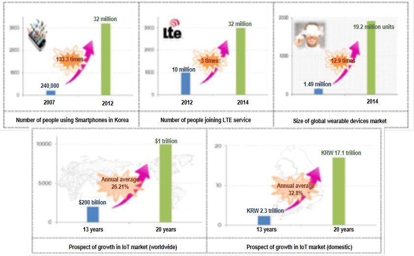
[Figure 2. Trend of increase in people using domestic Smartphone services, size of global wearable devices market, and prospect of growth on IoT. (Source: Ministry of Science, ICT and Future Planning ,2014)]
Status on electromagnetic interference technology (EMI)
When an electromagnetic contacts a conductor, it is reflected. Therefore, in order to shield electromagnetic waves that are produced, conductive materials need to be used. Metal materials in the forms of plate, mesh, and ionized gas are being used selectively according to the purpose of using the product and the required costs.
The methods of electromagnetic interference technology are twofold: one that protects external equipment by covering the surroundings of the electromagnetic origin and one that protects the equipment from external electromagnetic origin by putting it inside a covering material. Regarding such methods, studies on shielding materials for electromagnetic interference are gaining heated attention, but there remain many limitations in terms of capabilities, applicability, and costs of shielding materials.
1. Electromagnetic interference using sheet metal
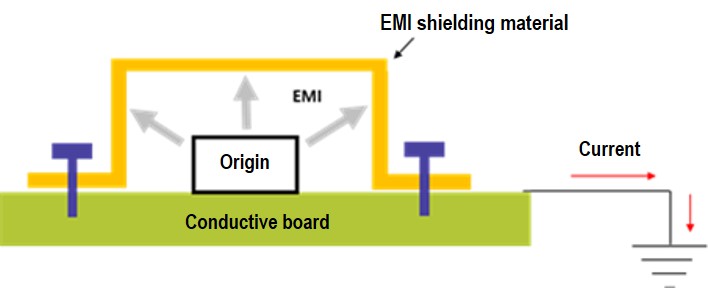
[Figure 3. Basic overview on EMI]
General method of EMI is to seal and ground the origin using metal plate (such as the power board in Figure 4). However, there are difficulties in using such method due to the structure of the products. For non-display units, major factors to consider include space and heating. For display units, preventing the decrease in image quality needs to be considered additionally.
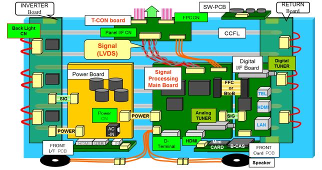
[Figure 4. Board Structure of existing LVDS (Low Voltage Differential Signal) LCD TV ]
2. Use of conductive thin-panel materials
In Figure 4, wired connector was used between T-con board and signal-processing main board of LCD TV. Along with increase in signal-processing speed and resolution, however, display noise due to EMI becomes a huge issue. Therefore, connector sealed using AI thin-panel material is used to prevent decrease in image quality.
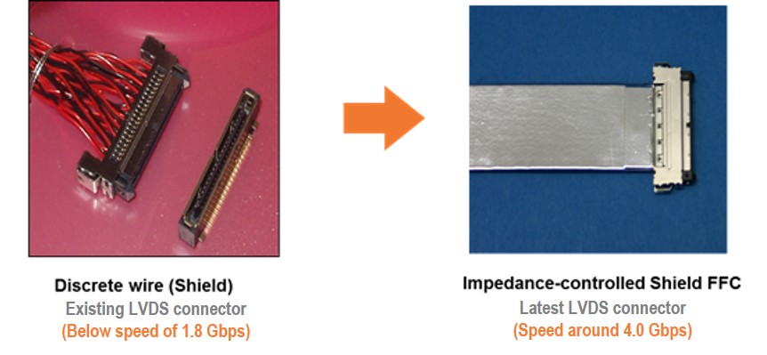
[Figure 5. EMI technology of LVDS for TV]
3. Use of conductive metalized film or metal mesh
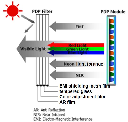
[Figure 6. Case of EMI for TV display unit Source : NNP technology]
As shown in Figure 6, PDP is an EMI shielding material which uses Ag metalized film or Cu mesh film. For display units of cell phones, ITO metalized film serves the function of EMI shielding. Low resistance is required for EMI shielding. For same materials, increased thickness leads to increased cross sectional area, reducing resistance.
In this case however, reduction in light transmission due to increased thickness becomes a problem. Therefore, materials with improved light transmission capability and sheet resistance are in demand.
Excellent EMI shielding capability of Graphene
Conductivity reflects electromagnetic wave to its reverse direction and magnetic force absorbs the energy of electromagnetic wave itself. Therefore, in EMI shielding, it is ideal to use thin and flexible shielding material which has both characteristics appropriately, while having transparency in some cases. Consequently, Graphene is gaining attention with its next-generation EMI shielding material which has high electrical conductivity, heat conductivity, flexibility, transparency, etc.
In Graphene, a magnetic field that is opposite to the external magnetic field is induced due to the fast-moving flow of electrons. This leads to a hundredfold shielding efficiency at most compared to shielding materials that rely on paramagnetic substances. Using various materials with graphene coating enables efficient shielding from approximately 2GHz to 18 GHz. The flexibility, transparency, and coating capability of graphene renders it appropriate to be used as EMI shielding material for wearable devices. Also, it can be used for developing functional contact lenses due to its antibacterial capability and EMI shielding characteristics.
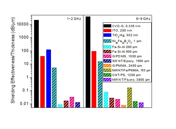
[Figure 7. Graph which shows the efficiency of graphene in shielding electromagnetic wave]
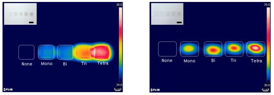
[Figure 8. Experiment on absorption of microwave by graphene. It absorbs strong electromagnetic wave energy and emits it as heat energy.]
EMI technology of Graphene Square
Graphene Square owns EMI technology and patent for transferring graphene inside or outside the electromagnetic origin. Using this technology which produces uniform graphenes with large area in same sizes, electromagnetic waves that occur from various electromagnetic origins can be shielded with efficiency. More specifically, various materials coated with graphene can shield electromagnetic waves from a broad range of frequency, from approximately 2 GHz to 18 GHz, while improving the efficiency of EMI shielding through chemical, physical, and structural improvements.
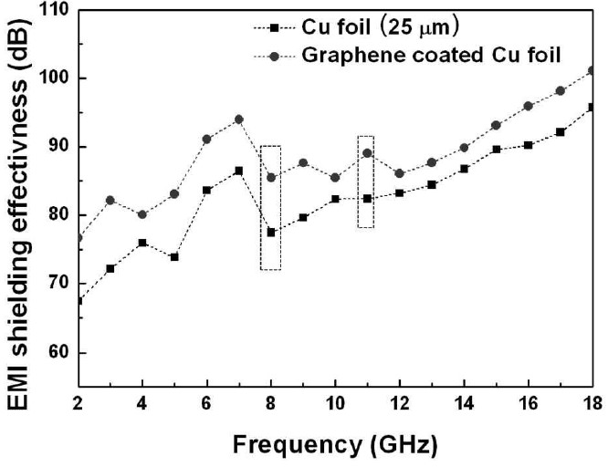
[Figure 9. Shielding efficiency of graphene]


