
How to make Graphene?
Graphene can be primarily produced by two main methodsTop-down method starting from graphite flake (micro flake) and bottom-up method from carbon precursors that could be decomposed to atomic carbon under synthetic conditions.
VIEW CVD EQUIPMENT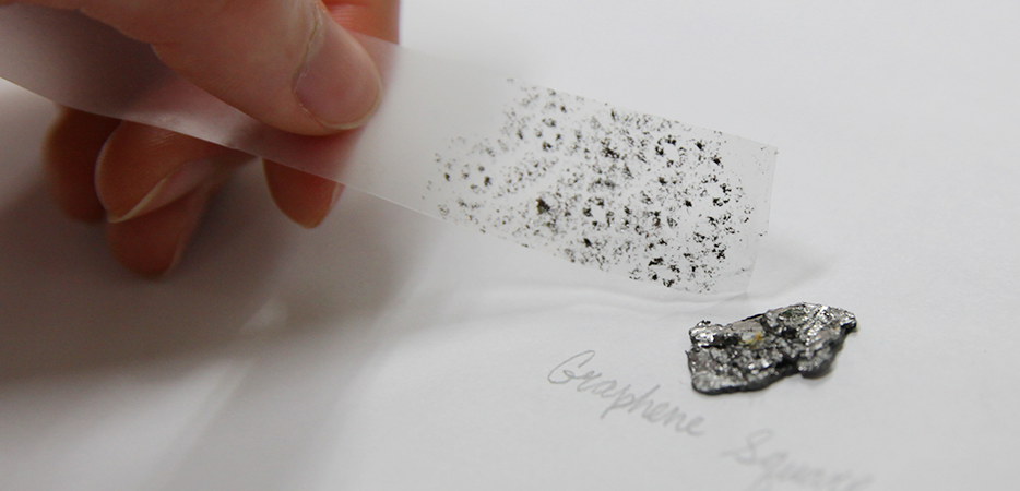
1. Top Down Method Graphene can be produced by exfoliation of bulk graphite including mechanical cleavage using Scotch tape, direct liquid phase exfoliation of graphite/ graphite intercalation compound with the help of ultrasonication or via oxidation of graphite to graphite oxide (GO), exfoliation of GO to graphene oxide by ultra sonication followed by reduction process to restore electronic propeties(reduced graphene oxide-RGO). Graphene produced from graphite by direct exfoliation methods have relative high crystal quality (high electrical conductivity, less crystal defect) but the production yield are still so low that is not enough for practical application. Product are usually contaminated by organic impurities and its is difficult to control the number of graphene layers (whereby increasing the number of layers decrease its optical transparency).
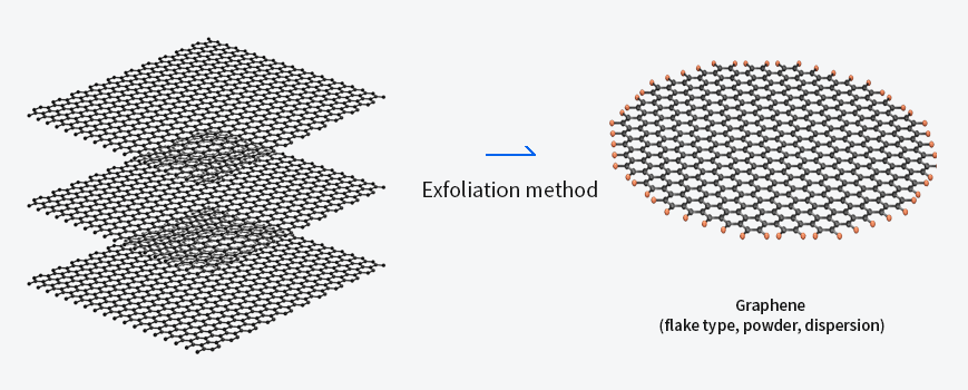
Graphene produced through oxidation of graphite to graphene oxide (GO), exfoliation of resulting GO and reduction of exfoliated graphene oxide (RGO) is the most popular method (Hummer's method). This method often yields of multi-layers graphene (RGO) in flake types which having lateral length in the range of several hundred nano meters to several micrometers. This method is suitable for mass production of graphene flakes with at relative low production cost and can yield large quantities of graphene flakes for variety of application, where high purity is not required such as fillers for polymer nanocomposites, coating, conductive ink paste, energy storage application (electrode for Lithium ion, Lithium sulfide, Lithium-air batteries and suppercapacitors) etc. But because of its flake type (several آµm in size) with high impurity is not suitable for flexible, large area transparent conductive electrode application in electronics.
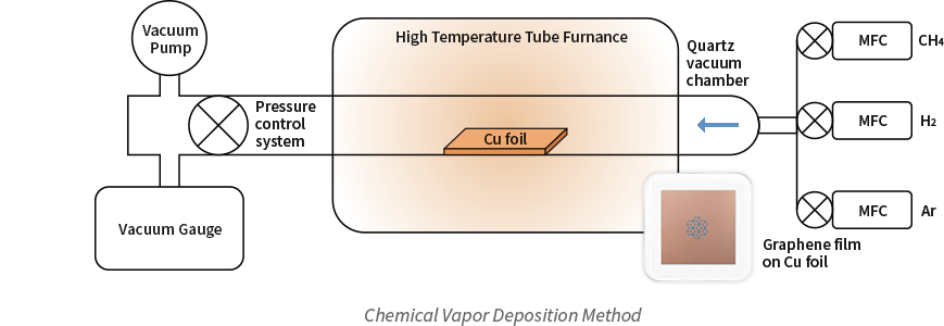
2. Bottom Up Method Graphene can be produced by molecular growth from small molecular carbon precursors by Chemical Vapor Deposition (CVD) or epitaxial grown on a substrate, where well controlled thickness (number of layers) can be done using different substrate catalysts and growing parameters. Graphene by CVD method have large area, high quality and this method has the best potential for mass production of high purity graphene.
Four DifferentMethods of Production
-
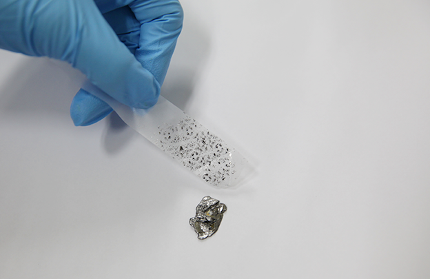 1) Mechanical Cleavage of HOPG
Commonly known as the Scotch-tape method, first developed by Novoselov and Geim in 2004 where an adhesive tape was used to detach graphene from graphite crystals. In the first peel, many layers of graphene were detached from graphite. In order to get monolayer, bilayers or few layers of graphene, the graphene is peeled repeatedly from the adhesive tape. Then finally the tape is att- ached to a substrate and glue is removed by dissolving it in solvent such as acetone.
-
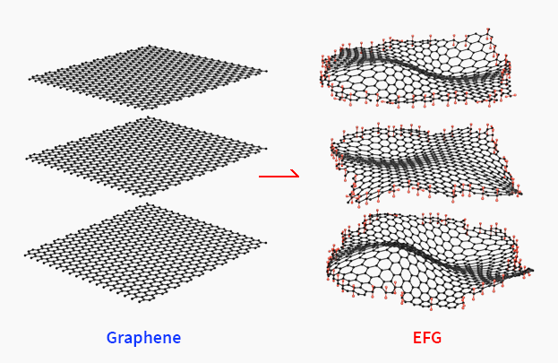 2) Solution Processing
Liquid Phase Chemical Exfoliation of Graphite is done by dispersing graphite in an organic solvent (0.3 mg/mL sodium cholate) with almost the same surface energy as graphite, so that the energy barrier is removed to facilitate the detachment of graphene layer. This solution is then either ultrasonicated for 100–400 hrs or voltage is applied to the solvent to split the graphite into individual graphene sheets as suspension. Then the solution is centrifuged between 500 and 2000 rpm to remove the thicker flakes. By this process, graphene flakes of 1–10 stacked monolayers with up to 20% of flakes containing just one layer is obtained.
-
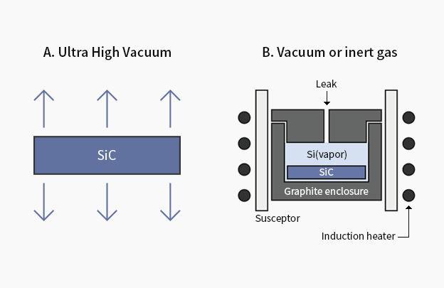 3) Epitaxial Growth on SiC Substrates
Silicon carbide wafer is used to produce epitaxial graphene by graphitization at high temperatures. At high temperature and ultra-high vacuum or atmospheric pressure,Si atoms sublime and remaining carbon forms graphitic lay ers on either carbon or silicon faces of SiC wafer. Methods have been developed to control the growth of the number of graphene layers.
-
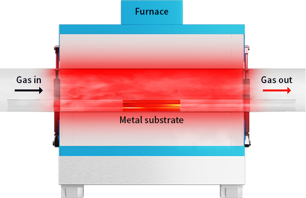 4) Chemical Vapor Deposition (CVD)
CVD is a bottom-up approach for the direct synthesis of graphene from carbon so urces or precursors such as methane, which is then transferred to a substrate. By CVD method large-area, single and few-layer graphene she ets are gro wn on metal foil substrates such as Cu foil. The grap hene sheet deposited on the Cu foil is then transferred to a dielectric surface or other substrates of int erest. By this method, square meters of monolayer graphene has been fabricated (Li et al. 2009) and transferred to a 200 mm Si wafer. It shows great promise for its use in touchscreens. CVD has the potential and promise to beco me a commercial technology.
* Currently, CVD is the only way to produce high quality, large scale graphene films .
Chemical Vapor Deposition at Graphene Square
CVD Growth of Large-Scale Graphene on poly-NiProf. Hong’s group pioneered the CVD synthesis of graphene . The corresponding Nature paper has been recording No. 1 citation rate in chemistry.
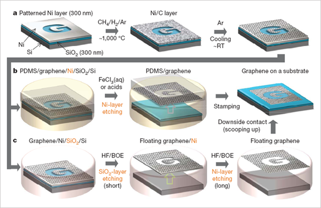 K.S. Kim et al. Nature 457, 706 (2009)
-
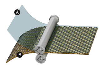
A. Polymer support B. Graphene on Cu foil
-
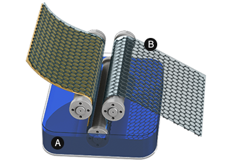

A. Cu etchant B. Graphene on polymer support
-
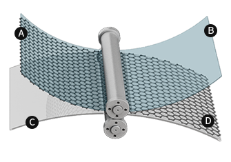

A. Graphene on polymer support B. Released polymer support C. Target substrate D. Graphene on target
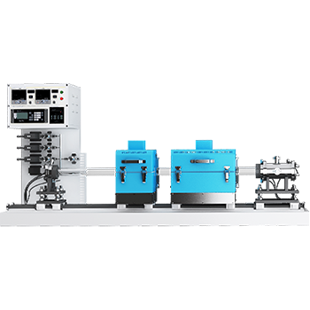
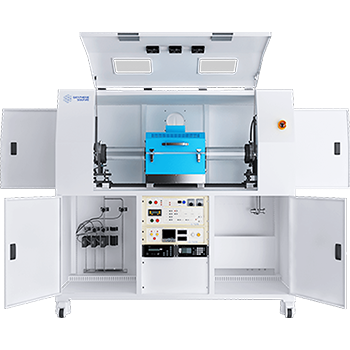
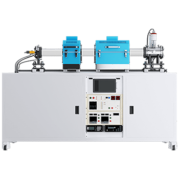
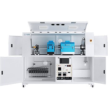
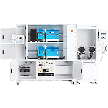
GSI developed a variety of CVD equipment that are suitable for lab research scale to industrial scale, enable producing high quality, excellent uniformity monolayer graphene as sample for basic studies including thermal TCVD-50B, dual zones halogen lamp TCVD-100A with rapid heating/ cooling and automated PC controllable Plasma Enhanced Chemical vapor deposition (TCVD-100CA) or 8 inches industrial Roll to Roll Chemical Vapor Deposition (TCVD-V200A)..ect.
GSI produced world best quality graphene film with excellent surface coverage (>95%), high carrier mobility (>3500 V.s-1m-1), low sheet resistance (250~400 خ©/sq), uniformity monolayer graphene on a variety of substrates such as flexible polyethylene terephthalate (PET), thin flexible glasses, SiO2 wafer, quartz glasses...etc are ready for commercialization in the sectors electronic applications. In parallel to developing graphene synthesis (CVD) equipment, GSI is also continuously R&D investing in improving graphene synthesis and transfer technology for lowering production cost and improving graphene quality.
| TCVD-50B | TCVD-100A | TCVD-D100CA | TCVD-RF100CA | TCVD-DRF100CA |
|---|---|---|---|---|
 |
 |
 |
 |
 |


