Recent advance in Graphene & 2D materials research for thermoelectric application
1. Introduction to thermoelectric materials.
Thermoelectric materials (TEM) have been a promising technology for producing electricity from heat that would otherwise just be wasted. Thermoelectric research has regained renewed attention recently because of the huge potential of TEM to be applied in Peltier coolers and thermoelectric power generators.
The thermoelectric effect is the phenomena by which either a temperature difference creates an electric potential or an electric potential creates a temperature difference. As for all heat engines, the efficiency of a thermoelectric system with a hot end at temperature Th and a cold end at temperature Tc should reach the theoretical Carnot efficiency خ·Carnot = 1 - Tc/Th if the thermoelectric cycle was fully reversible. However, it is practically limited by irreversible losses, i.e. the loss due to Joule heating and the thermal conduction, and by the thermoelectric properties of the material. The maximum efficiency of a thermoelectric system can be written as [1]:

Where, ZT is a dimensionless parameter that measures the performance of the thermoelectric material (also called thermoelectric figure of merit).
A basic description of thermoelectrics usually involves two reciprocal processes: the Seebeck and Peltier effects. The Seebeck effect is the generation of a voltage due to a temperature difference and is quantified by the Seebeck coefficient or thermopower of a material, S=-خ”V/خ”T, used for temperature sensing in thermocouples.
It is well known that the thermoelectric (TE) effect is existed in most materials, but very few materials have a large enough TE effect for practical applications. A good thermoelectric material must involve a high Seebeck coefficient and excellent electrical conductivity, as well as low thermal conductivity. The thermoelectric figure of merit ZT (eq.1) is normally used to indicate the energy conversion efficiency.
ZT=دƒS2T/خ؛ (1)
Where S is the Seebeck coefficient (or thermopower, خ¼V/K), دƒ is the electronic conductance (S/m), k (خ؛ = خ؛e + خ؛p) is the thermal conductivity including contributions from both phonons and electrons (W/mK), and T is the absolute temperature (K).
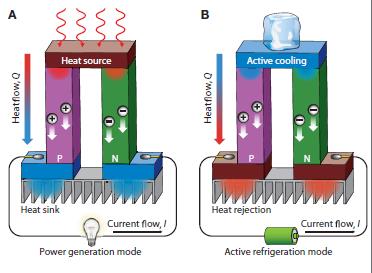
Figure 1 shows a schematic illustration of a thermoelectric module for (a) power generation (Seebeck effect) and (b) active generation (Peltier effect). Figure 1A shows an applied temperature difference, which causes charge carriers in the material (electron or holes), to diffuse from the hot side to the cold one, resulting in a current flow through the circuit. Figure 1B is schematic of the heat that evolves at the upper junction and is adsorbed at the lower junction when a current is made to flow through the circuit.

Figure 1. Schematic illustration of a thermoelectric module for (A) power generation (seebeck effect) and (B) active generation (Peltier effect)[2]
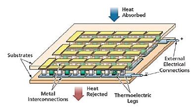
Good TE materials should exhibit an outstanding TE effect which can be used in applications including power generation, refrigeration, and most importantly waste heat recycling [1-3]. Figure 2 show a typical structure of a commercial Bi2Te3 thermoelectric generator [3].

Figure 2: Structure of a commercial Bi2Te3 thermoelectric generator [3]
The challenge to develop high performance TEM for a crystalline system is know how to tailor the interconnected thermoelectric physical parameters, including Seebeck coefficient, electrical conductivity and thermal conductivity.
Therefore, it is important to know some basic principles on the selection of materials suitable for thermoelectrics. Generally, a large Seebeck coefficient is usually found in low carrier concentration semiconductors while a large electrical conductivity is found in high carrier concentration metals. To maximize the power factor دƒS2, the best compromise is to use heavily doped semiconductors. In fact, in a semiconductor with a finite bandgap, electrons and holes can be separated and doping produces a high density of a single carrier type so that the Seebeck coefficient is not reduced by opposite contributions of electrons and holes. Thus, good thermoelectric materials have a bandgap large enough to have only a single type of carrier but small enough to make a high doping level possible, to achieve high electrical conductivity.
Among the materials selected to offer the best compromise, PbTe, Bi2Te3 and their alloys were found since the 1950s to provide high values of ZT [4, 5], which motivated the creation of the thermoelectric industry. However, over the following three decades, only small advancement were achieved in increasing ZT, to such a point that the thermoelectrics community tended to consider the value of about 1 as an upper limit for ZT. If we except the progress made in skutterudite materials [6] and in Half-Heusler alloys [7], the best thermoelectric material was found in the (Bi1-x Sbx)2 (Se1-yTey)3 alloy family, with ZT ? 1 at room temperature. This class of commercially available materials currently dominates in temperature control and thermal management applications. However, in some cases when attempting to recycle waste heat from diverse sources, reasonable conversion efficiency is difficult to be realized using these types of materials [8]. It is well known that the lower flexibility and ductility of bismuth telluride and it alloys leads to difficulty combining it with the current types of small portable devices such as mobile phones and laptop computers, not to mention some future devices involving irregular surfaces or flexible substrates. Another disadvantage of bismuth telluride-based TE materials is that these materials are not transparent. In other words, these materials cannot be applied on the windows glass of buildings or vehicles, which are good power sources for temperature-to-electricity conversion since a large temperature difference normally exists on the two sides of the glass.
Until now the slow growth of the thermoelectrics industry was based the fact that only niche applications were developed for which cost and energy efficiency were not important issues. A value of ZT ? 3 is desirable to broaden the use of thermoelectric solid state devices by making them competitive with conventional mechanical energy conversion systems.
A renewal of thermoelectrics material research came in the 1990s from the pioneering works of Hicks and Dresselhaus [9] who suggesting that nanostructuring materials into two-dimensional (2D) systems should provide much higher ZT (>1) and thermoelectric efficiencies than with bulk materials. This enhancement of ZT in low-dimensional systems has two main origins, i.e. (i) the Seebeck coefficient enhancement resulting from size-quantization and (ii) the reduction of phonon thermal conductivity due to interface effects.
2. Recent advance in research on thermoelectric effect in Graphene
Graphene, a two-dimensional (2D) allotrope of carbon, has attracted much attention due to its superior electrical, mechanical and thermal properties [10~12]. Due to superior high carrier mobility and it possibility to create a bandgap by physical defect or chemical doping, graphene have been continuously attracting tremendous attention from academic as well as industrial researchers and scientists.
Graphene [10~11] has been shown theoretically and experimentally [12~17] to have a large and tunable thermopower (S) up to آ±100خ¼VK-1 at room temperature, due to its unique electronic band structure and electrostatic tunability of the density and polarity of its charge carriers. In contrast, the Peltier effect describes the heating or cooling of a junction between two different materials when an electric charge current is present. It is quantified by the Peltier coefficient خ , which can be understood as the heat transported by thermally excited charge carriers. The Peltier effect is a reversible thermodynamic phenomenon that depends linearly on the current, so it is fundamentally different from the irreversible Joule heating. More importantly, as both thermoelectric coefficients are related by the second Thomson relation خ =ST, where T is the reference temperature, it follows that in graphene also the Peltier coefficient خ (and its associated cooling or heating action) can be controlled in both magnitude and sign.
The thermoelectric power (TEP) is the voltage developed across a sample when a constant temperature gradient is applied. TEP of 80 خ¼V/K was recently measured in graphene at room temperature (300 K)[18]. Similar to the quantum Hall effect in electronic transport, quantized TEP has also been observed in graphene at high-magnetic fields [18]. The TEP can be tuned in graphene, even to negative values, under the application of a gate bias or chemical potential [19]. Very large TEP values have been predicted for GNRs, for instance, 4 mV/K for a 1.6 nm wide ribbon [20]. In comparison, the highest value experimentally reported so far is 850 خ¼V/K for two-dimensional electron gases in SrTi2O3 heterostructures [21] while only a few خ¼V/K has been reported for bulk graphite [22]. The TEP power of single walled carbon nanotubes (SWNTs) has been theoretically and experimentally shown to be 60 خ¼V/K [23] inferior to that of graphene. A giant thermoelectric coefficient of 30 mV/K was reported in metallic electrodes periodically patterned over graphene, deposited on SiO2 substrate [24].

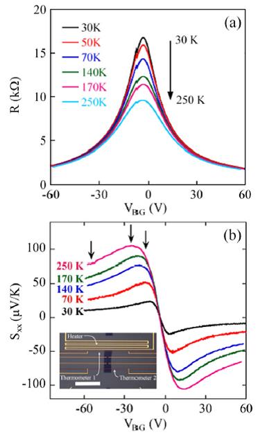
Figure 3. Thermoelectric measurements in bilayer graphene. (a)Two-terminal resistance R and (b) thermopower as a function of the backgate voltage VBG in zero magnetic field and at various temperatures: T = 30, 50, 70, 140, 170, and 250 K. Inset: optical image of a typical device. Size of the scalebar is 30 nm [25]
Various structures of graphene have been examined, including nanoribbons (GNRs)[20], quantum dots [26], graphene junctions, and chevron-type structures [27]. It is worth noted here that ZT of zigzag GNRs can exceed 3 [28].
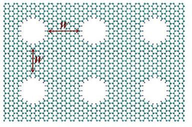
Recently, many works have been conducted on the creation of graphene band gap by means of making an array of holes (antidots) into the graphene layer. This is an inevitable property for the integration of graphene material directly into transistor architecture. The gap can be engineered by controlling the lattice geometry (i.e., the antidot size and the hole-to-hole separation) . Further, thermoelectric properties of these structures (2D graphene antidot lattices) have also been investigated where ZT up to 0.3 was found [29] (see Fig.4).

Figure4. A typical H-passivated GNM system. Here the big cyan (small blue) spheres represent C (H) atoms, and W denotes the neck width along the zigzag and armchair directions
1. Thermoelectric in other 2D materials beyond graphene.
Since the discovery of graphene and of the â€کwonderful world’ of 2D layered materials, plenty of new 2D materials were proposed and unveiled, such as graphene oxide, hybrid hydrogenated graphene (in the form of graphane or graphone), hexagonal boron nitride (BN) monolayers, hybrid graphene/BN monolayers, thallium nitride monolayers, aluminium nitride monolayers, germanium carbide monolayers, gallium nitride monolayers, silicene, phosphorene, molybdenum disulfide, and other transition metal dichalcogenides. New forms of non-natural carbon allotropes related to graphite/graphene, graphyne and graphdiyne have also been the subjects of interest due to their unique structures and intriguing properties. Here, we review some of the most promising of them in terms of thermoelectric properties.
From Density Functional Theory- Keldysh non-equilibrium Green’s function (DFT-NEGF) simulation, Ni et al have found that the thermoelectric properties of armchair graphane nanoribbons (AGANRs) are higher than those of AGNRs and further enhanced in the presence of disorder [30]. By introducing disorder in the form of imperfect saturation of the hydrogencarbon bonds, the authors have shown that the lattice thermal conductance is reduced without drastically affecting the electric conductance, which results in the high figure of merit ZT=2.1 at room temperature and ZT > 3 at T = 700 K. Higher value ZT=5.8was even predicted for 5 nm-wide ribbons under appropriate disorder conditions.
In a hetero-structure system, a zigzag ribbons consisting of a graphene/BN heterostructrue is predicted to have a very high Seebeck coefficient with an enhancement by a factor of 20 compared to graphene [31]
Interestingly, monolayers of transition metal dichalcogenides (MX2 compounds with M=Mo,W, and X=S, Se, or Te), are atomically thin 2D semiconductors with a finite bandgap, have been the recent focus of extensive research activity both fundamental physical properties as well it thermoelectric properties.
By means of non-equilibrium molecular dynamics simulation, Liu et al have shown that the thermal conductivity of monolayer MoS2 is only 1.35WmK-1 at room temperature, which is three orders of magnitude lower than that of graphene [32]. In contrast to the case of GNRs, the thermal conductivity of monolayer MoS2 nanoribbons (NRs) is insensitive to width and edge-type, indicating that the phonons Umklapp scattering process dominates the thermal transport in MoS2 NRs. Experimentally, by scanning photocurrent spectroscopy of MoS2 transistors, it has been shown that the Seebeck coefficient of single-layer MoS2 can be tuned by an external electric field between -4 أ— 102 and -1 أ— 105 خ¼VK-1 [33]. Combining this high value of thermopower with the low thermal conductivity mentioned above, one may expect good thermoelectric performance. From first-principles DFT calculation, Huang et al have investigated the thermoelectric performance of different kinds of dichalcogenide monolayers, including MoS2, MoSe2, WS2 and WSe2 [34]
Example, at high temperature, n-type WSe2 shows an exceptional increasing rate compared to other cases, due to the electron transport contribution of an additional valley, leading to ZT > 1 at T = 500 K. The same authors have shown that ZT = 2.1 is achievable in bilayer WSe2 at room temperature [35].
Phosphorene, another 2D materials discovered recently after graphene, based on first principles calculation, Fei et al have found that the electrical and thermal conductance exhibit strong spatial anisotropies such that their respective preferred directions of conductance are orthogonal to one another, resulting in an anisotropic thermoelectric figure of merit that is large along the armchair direction [36]. By considering a phonon relaxation time of 60 ps, ZT has been predicted to reach more than 1 at room temperature and 2.5 at T = 500 K. Lv et al have shown that strain-induced band convergence in phosphorene can significantly enhance simultaneously the Seebeck coefficient and electrical conductivity, which leads to ZT = 2.1 at room temperature in the armchair direction [36].
2. Conclusion.
Although most current research on graphene &2D materials in thermoelectric are based on theoretical calculation or simulated predictions, it still need to be confirmed by the experimentalist, they show clearly that graphene and similar atomically thin layered 2D materials such as transitional metal dichalcogenides and phosphorene are very promising for future development of thermoelectric energy conversion at the nanoscale. Due to the high sensitivity of most physical properties of these materials to atomic defects and to the environment, a significant obstacle is obviously the fabrication of well-controlled nanostructures. However, the recent progress achieved in the bottom-up synthesis of graphene nanoribbons with atomically precise edges makes it realistic to envision in the near future the experimental demonstration of some fascinating results recently predicted by numerical simulations.
3. References
[1]. Philippe Dollfus, Viet Hung Nguyen and Jerome Saint-Martin, Thermoelectric effects in graphene nanostructures, J. Phys.: Condens. Matter 27 (2015) 133204 (20pp).
[2]. Li, J. F., et al. High-performance nanostructured thermoelectric materials, NPG Asia Mater. 2, 152-158
[3]. Ramadass, Y. K., & Chandrakasan, A. P. (2011). “A Battery-Less Thermoelectric Energy Harvesting Interface Circuit With 35mV Startup Voltageâ€. IEEE Journal of Solid-State Circuits, 46(1), 333-341
[4]. Goldsmid H J, Sheard A.R. and Wright D.A. 1958 The performance of bismuth telluride thermojunctions Br. J. Appl. Phys. 9, 365-70
[5] Ioffe A.F. 1957 Semiconductor Thermoelements, and Thermoelectric Cooling (London: Infosearch Ltd.)
[6]. Shi X, Yang J, Salvador J R, Chi M, Cho J Y, Wang H, Bai S,Yang J, Zhang W and Chen L 2011 Multiple-filled skutterudites: high thermoelectric figure of merit through separately optimizing electrical and thermal transports, J. Am. Chem. Soc. 133 7837-46
[7]. Culp S R, Simonson J W, Poon S J, Ponnambalam V, Edwards J and Tritt T M 2008 (Zr,Hf)Co(Sb,Sn) half-Heusler phases as high-temperature (>700 ℃) p-type thermoelectric materials. Appl. Phys. Lett. 93 022105.
[8]. Vining CB. An Inconvenient Truth About Thermoelectrics. Nature Materials. 2009, 8(2):83-5.
[9]. Hicks L D and Dresselhaus M S 1993 Effect of quantum-well structures on the thermoelectric figure of merit. Phys. Rev. B, 47, 12727-31
[10]. Castro Neto, A. H., Guinea, F., Peres, N. M. R., Novoselov, K. S. & Geim, A. K. The electronic properties of graphene. Rev. Mod. Phys. 81, 109-162 (2009).
[11]. Das Sarma, S., Adam, S., Hwang, E. H. & Rossi, E. Electronic transport in two-dimensional graphene. Rev. Mod. Phys. 83, 407-470 (2011).
[12]. Ouyang, Y. & Guo, J. A theoretical study on thermoelectric properties of graphene nanoribbons. Appl. Phys. Lett. 94, 263107 (2009).
[13]. Yan, X.-Z., Romiah, Y. & Ting, C. S. Thermoelectric power of Dirac fermions in graphene. Phys. Rev. B 80, 165423 (2009).
[14]. Hwang, E. H., Rossi, E. & Das Sarma, S. Theory of thermopower in two-dimensional graphene. Phys. Rev. B, 80, 235415 (2009).
[15]. Zuev, Y. M., Chang, W. & Kim, P. Thermoelectric and magnetothermoelectric transport measurements of graphene. Phys. Rev. Lett. (2009), 102, 096807
[16]. Wei, P., Bao, W., Pu, Y., Lau, C. N. & Shi, J. Anomalous thermoelectric transport of dirac particles in graphene. Phys. Rev. Lett. (2009), 102, 166808.
[17]. Checkelsky, J. G. & Ong, N. P. Thermopower and Nernst effect in graphene in a magnetic field. Phys. Rev. B 80, 081413 (2009).
[18]. Zuev, Y. M., Chang, W., and Kim, P.. Thermoelectric and magnetothermoelectric transport measurements of graphene. Phys. Rev. Lett. 2009, 102, 096807.
[19]. Wei, P., Bao, W., Pu, Y., Lau, C. N., and Shi, J. Anomalous thermoelectric transport of dirac particles in graphene. Phys. Rev. Lett. (2009), 102, 166808.
[20] Haskins, J., Kؤ±nacؤ±, A., Sevik, C., Sevincli, H., Cuniberti, G., and Ca?ؤ±n, T. A theoretical study on thermoelectric properties of graphene nanoribbons. Appl. Phys. Lett. (2009), 94, 263107.
[21]. Ohta, H., Kim, S., Mune, Y., Mizoguchi, T., Nomura, K., Ohta, S., et al.. Giant thermoelectric Seebeck coefficient of a two-dimensional electron gas in SrTiO3. Nat. Mater. (2007), 6, 129-134.
[22]. Tyler, W.W. and Wilson, A.C. Thermal conductivity, electrical resistivity, and thermoelectric power of graphite. Phys. Rev. (1953). 89, 870-875.
[23]. Hone, J., Ellwood, I., Muno, M., Mizel, A., Cohen, M. L., Zettl, A., et al., Thermoelectric power of single-walled carbon nanotubes. Phys. Rev. Lett. (1998). 80, 1042-1045.
[24]. Chang, P.H. and Nikolic, B.K. Giant thermoelectric effect in graphene. Appl. Phys. Lett. (2007). 91, 203116.
[25]. Nam S-G, Ki D-K and Lee H-J 2010 Thermoelectric transport of massive Dirac fermions in bilayer graphene. Phys. Rev. B, 82 245416.
[26]. Yan, Y., Liang, Q.-F., Zhao, H., and Wu, C.-Q. (2012). Thermoelectric properties of hexagonal graphene quantum dots. Phys. Lett. A, (2012), 376, 1154-1158
[27]. Chen, Y., Jayasekera, T., Calzolari, A., Kim, K. W., and Nardelli, M. B. (2010b). Thermoelectric properties of graphene nanoribbons, junctions and superlattices. J. Phys. Condens. Matter. 22, 372202
[28]. Ouyang, T., and Hu, M. (2010). Enhanced thermoelectric figure of merit in edge-disordered zigzag graphene nanoribbons. Phys. Rev. B, (2010), 81, 113401.
[29]. Oswald W and Wu Z, Energy gaps in graphene nanomeshes. Phys. Rev. B, (2012) 85, 115431
[30]. Ni X, Liang G, Wang J-S and Li B, Disorder enhances thermoelectric figure of merit in armchair graphene nanoribbons. Appl. Phys. Lett. (2009), 95 192114
[31]. Yokomizo Y and Nakamura J , Giant Seebeck coefficient of the graphene/h-BN superlattices, Appl. Phys. Lett. (2013), 103, 113901
[32]. Liu X, Zhang G, Pei Q-X and Zhang Y-W, Phonon thermal conductivity of monolayer MoS2 sheet and nanoribbons, Appl. Phys. Lett. (2013),103, 133113
[33]. Buscema M, Barkelid M, Zwiller V, van der Zant H S J, Steele G A and Castellanos-Gomez A, Large and tunable photothermoelectric effect in single-layer MoS2, Nano Lett. (2013), 13, 358-63
[34]. Huang W, Da H and Liang G 2013 Thermoelectric performance of MX2 (M = Mo,W; X = S,Se) monolayers J. Appl. Phys.(2013) 113, 104304
[35]. Huang W, Luo X, Gan C K, Quek S Y and Liang G, Theoretical study of thermoelectric properties of few-layer MoS2 and WSe2 Phys. Chem. Chem. Phys. (2014), 16, 10866-74
[36]. Lv H Y, Lu W J, Shao D F and Sun Y P, Enhanced thermoelectric performance of phosphorene by strain-induced band convergence Phys. Rev. B (2014), 90, 085433


