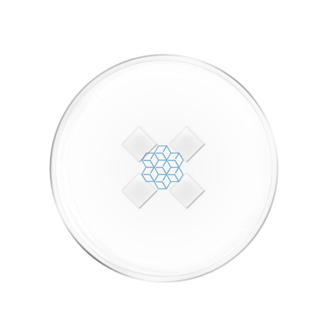
Orderآ Sizeآ large areaآ alsoآ available
Product and Service Overview
The state of the art chemical vapor deposition (CVD) method is used to synthesize our high-quality graphene products. It boasts more than 90% coverage of mono-layer graphene.
We also provide various studies and measurements on graphene samples to meet your need for high-end research and application.
-
Properties
- Product Size : Up to 140x140mm2(8" wafer)
- Film morphology : Continuous Monolayer(>95%)
- Sheet Resistance : Av. < 250~400 خ©/sq (after transfer)
- Mobility : >3500cm2/Vs (Max. 17.000 cm2/Vs)
- Transmittance : >97%
- Subtrate : Quartz plate (1T) (Standard)
- Domain Size:~10مژ›
-
Quartz plate Specifications
ى‚°ى†Œ, ىˆکى†Œى—°ىڑ©ë²•ىœ¼ë،œ ى„ىکپى¸ê³ يٹ¸ë¥¼ ىƒى‚°ي•کى—¬, يˆ¬ëھ…ى„ىکپى›گيŒگ, ى‚¬ê°پيŒگ, FLANGE 등ىœ¼ë،œ 가공ي• ىˆک ىˆê³ , ىœˆëڈ„ىڑ°, ë°کëڈ„ى²´, ى„ىکپ부ي’ˆ 등ىک ى¬ë£Œë،œ ى‚¬ىڑ©ëگ©ë‹ˆë‹¤.
OH 가공ي•¨ëں‰ : 120~260 ppm
Flame fused ingots are re-heated to make many shaped plates. This plates can be used for window material, mask substrate and flanges.
Another hand the ingot is drawn to rod for quartz boat, fabrication welding rod and optical fiber parts.
OH contents will be 120~260 ppm as generalChemical element composition (Typical data)
Al Fe K Li Cu NaS B Ca Mg P Ti OH 20.00 0.40 1.00 1.4 0.01 1.50 0.20 0.50 - - - 120-260 Transparent quartz glass property
- 비ى¤‘(Density) 2.21x10³ kg/m3
- 비ى¤‘(Density) 2.21x10³ kg/m3
- 비ى¤‘(Density) 2.21x10³ kg/m3
- 비ى¤‘(Density) 2.21x10³ kg/m3
- 비ى¤‘(Density) 2.21x10³ kg/m3
- 비ى¤‘(Density) 2.21x10³ kg/m3
- 비ى¤‘(Density) 2.21x10³ kg/m3
- 비ى¤‘(Density) 2.21x10³ kg/m3
Optical property
يˆ¬ëھ… ى„ىکپ ى¬ë£Œëٹ” ى¢‹ى€ يˆ¬ê³¼ىœ¨ى„ ê°–ê³ ىˆىœ¼ë©°, يٹ¹يˆ ى پى™¸ى„ ê³¼ ê°€ى‹œê´‘ى„ يˆ¬ê³¼êµ¬ê°„ى—گى„œ ى„ىکپىœ 리ëٹ” ى¼ë°ک ىœ 리보다 يˆ¬ê³¼ىœ¨ى´ ي›¨ى”¬ 높ىٹµë‹ˆë‹¤.
ى پى™¸ى„ ىک يˆ¬ê³¼ىœ¨ê³¼ 금ى„불ىˆœë¬¼ى€ ë°€ى ‘ي•œ 관계가 ىˆىٹµë‹ˆë‹¤. 2730nmى—گى„œ OHىک ي،ىˆکê°€ ى œى¼ 높ىٹµë‹ˆë‹¤.Our transparent quartz material has excellent transmission, especially ultra-red zone and visible area compare with ordinary glass.
Transmission of UV is related with metal impurities. 2730nm wave indicate OH content absorption and volume. -
Main target
For those researchers who do not have much experience in Graphene transfer process
For those researchers in need of graphene transfer onto transparent and flexible circuit board
For those researchers in need of high quality Graphene on Quartz glass
-
Additional options
- •Reduce sheet resistance by BI doping.
- •Reduce sheet resistance by Multi-layers graphene (Graphene stacking, laminated). (ex. 2, 3, 4, …, 10-layers)
- •Various sizes.
- •Transfer graphene onto Electrode patterned boards.
Measurement data
Our CVD grown graphene is uniformly distributed with excellent-
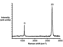
Raman Spectrum (after transfer)
-
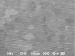
High-Revolution SEM Image
-
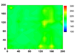
Sheet Resistance Uniformity
-
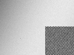
High-Revolution TEM Image
-
1
S. Bae*, H. Kim* et al. Roll-to-roll production of 30 inch graphene films for transparent electrodes Nature Nanotech. 5, 574 (2010).
-
2
Y. Lee et al. Wafer-Scale Synthesis and Transfer of Graphene Films. Nano Lett. 10, 490-493 (2010).
-
3
S. J. Kim*, T. Choi*آ et al.آ "Ultra-Clean Patterned Transfer of Single-Layer Graphene by Recyclable Pressure Sensitive Adhesive Films" آ Nano Lettersآ 15, 3236–3240 (2015)
Customer List
| National University of Singapore | Sabanci University |
| Nokia Research Center | Korea Basic Science Institute |
| HRL Laboratories | Seoul National University |
| LG Display | SungKyunKwan University |
| Korea Advanced Institute of Science andآ Technology | University of Bari Aldo Moro |
| Korea Atomic Energy Research Institute | Agency for Defense Development |
-
Graphene Square Advantages
-
World’s first large scale graphene synthesis towards commercialization.
Nature Nanotechnology 2010 cover image.
-
Many years of know-how in transfer method.
Coverage at above 95%, low residue. Most optimized R&D environment.
-
Our sample package is designed to minimize graphene damage.
Vacuum packaged, nitrogen filled. Easy to handle.
-
Optimized Graphene
We give advice and make suggestions to the beginners in graphene research. Offer Graphene on various and unique substrates.
-
Our commitment
We promise to deliver a level of quality unmatched and to our customers’ satisfaction.
-
All about Graphene-from thermal CVD equipment to graphene synthesis and transfer process with know-how.
Understanding of the whole process from the graphene synthesis, transfer, proper packaging with sound research is our key to success.
-
-
Delivery Packaging Process
- 01 Vacuum packaging, nitrogen filled
-
 02
Air cushion packaging
-
 03
Ready for pick up by
courier service
Order processOrder process  Customer order and payment confirmation
 Produce graphene
 Packaging
 Delivery
Status Review and confirm customer order Produce and inspect for high quality product Expert and protective packaging for S&H Estimated time of delivery is three business days Detailed shipment tracking on fedex.com -
FAQ
-
I would like to know Graphene Square’s graphene synthesis and transfer process.
1) Graphene synthesis process by Thermal CVD equipment
2) PMMA coating
3) Back side etching (using RIE)
4) Cu foil etching using APS solution
5) Rinse using DIW water
6) Transfer onto substrate, dry by baking on hot plate
7) Remove PMMA by dipping in Acetone
8) Quality check (Optical microscope, Raman spectroscope)
9) Vacuum package, shipping -
Are you able to offer CVD Graphene on Cu foil in sizes besides what is currently being offered?
Currently, the smallest size we offer [TCVD Graphene on Cu foil] is 50x50mm while the larger size offered is 80x80mm. If you are in need of smaller sizes then what we offer, we suggest that you purchase a 50x50mm and cut into required sizes. If you need sizes larger then 80x80mm, then you can send and email to below email address. info@graphenesq.com
-
I am handling graphene for the first time and I am trying to start with graphene on substrates (SiO2/Si wafer, glass, PET,,,). Please advise.
It may be possible to purchase graphene on Cu foil and do the transfer process even as a beginner, however, there may be multiple trial and error processes. As a result, we would suggest purchasing our graphene transferred on substrates or if you are in need of our graphene transfer service, we can provide such service customers’ substrate as well. < Custom Made Order link >
-
For Stacked graphene, is the transfer process done after PMMA coating of each layer? If not, what is the transfer process for Stacked graphene?
For multiple layers, we use graphene on Cu foil to initiate and perform overlapping process. The basic process is as follows: take [Graphene/Cu foil] and scoop from underneath [PMMA/Graphene] using DI water bath resulting in [PMMA/Graphene/Graphene/Cu foil]. Afterwards, Cu foil can be etched away and the above process can be repeated to make multiple layers of graphene.
-
Can graphene be mixed and used to make products using product molds or presses?
As you may know, graphene can be acquired in two methods. 1) Top down: mechanically exfoliating carbon from graphite to make graphene powder or graphene oxide, 2) Bottom up: since carbon is composed of gas (ex. CH4, C2H4,,,) graphene film can be synthesized at high temperature through the CVD method. One of the options can be considered depending on the research goals. Due to graphene’s characteristics, the theoretical prices and actual sample prices can vary and the characteristics of graphene powder and graphene film differ as well. As a result, when mixing graphene with other materials, graphene powder may be more appropriate. You would have to perform tests to find the right mixture ratios, but generally, mixing graphene powder with other materials to further manufacture products using molds or presses are possible.
-
How can I make graphene samples on substrates using dry transfer method?
For dry transfer, there are two main options: 1) Thermal release tape [TRT], 2) Pressure Sensitive Adhesive Film [PSAF]. The common requirement is that both methods require pressure using a laminator.
1) TRT: apply TRT with level pressure and temperature (100~110℃) simultaneously so that graphene can be released from the base surface of TRT onto the target substrate [based upon long period of experience and know-how, TRT is the suggested option versus PSAF].
2) PSAF: apply PSAF with level pressure from the base surface of PSAF onto the target substrate.
-
I would like to know Graphene Square’s graphene synthesis and transfer process.
1) Graphene synthesis process by Thermal CVD equipment
2) PMMA coating
3) Back side etching (using RIE)
4) Cu foil etching using APS solution
5) Rinse using DIW water
6) Transfer onto substrate, dry by baking on hot plate
7) Remove PMMA by dipping in Acetone
8) Quality check (Optical microscope, Raman spectroscope)
9) Vacuum package, shipping
-
Are you able to offer CVD Graphene on Cu foil in sizes besides what is currently being offered?
Currently, the smallest size we offer [TCVD Graphene on Cu foil] is 50x50mm while the larger size offered is 80x80mm. If you are in need of smaller sizes then what we offer, we suggest that you purchase a 50x50mm and cut into required sizes. If you need sizes larger then 80x80mm, then you can send an email request to below email address. info@graphenesq.com
-
I would like to know Graphene Square’s graphene synthesis and transfer process.
1) Graphene synthesis process by Thermal CVD equipment
2) PMMA coating
3) Back side etching (using RIE)
4) Cu foil etching using APS solution
5) Rinse using DIW water
6) Transfer onto substrate, dry by baking on hot plate
7) Remove PMMA by dipping in Acetone
8) Quality check (Optical microscope, Raman spectroscope)
9) Vacuum package, shipping
-
I am handling graphene for the first time and I am trying to start with graphene on substrates (SiO2/Si wafer, glass, PET,,,). Please advise.
It may be possible to purchase graphene on Cu foil and do the transfer process even as a beginner, however, there may be multiple trial and error processes. As a result, we would suggest purchasing our graphene transferred on substrates or if you are in need of our graphene transfer service, we provide such service on customers' substrates as well. < Custom Made Order link >
-
I would like to know Graphene Square’s graphene synthesis and transfer process.
1) Graphene synthesis process by Thermal CVD equipment
2) PMMA coating
3) Back side etching (using RIE)
4) Cu foil etching using APS solution
5) Rinse using DIW water
6) Transfer onto substrate, dry by baking on hot plate
7) Remove PMMA by dipping in Acetone
8) Quality check (Optical microscope, Raman spectroscope)
9) Vacuum package, shipping
-
Can graphene be mixed and used to make products using product molds or presses?
As you may know, graphene can be acquired in two methods. 1) Top down: mechanically exfoliating carbon from graphite to make graphene powder or graphene oxide, 2) Bottom up: since carbon is composed of gas (ex. CH4, C2H4,,,) graphene film can be synthesized at high temperature through the CVD method. One of the options can be considered depending on the research goals. Due to graphene’s characteristics, the theoretical prices and actual sample prices can vary and the characteristics of graphene powder and graphene film differ as well. As a result, when mixing graphene with other materials, graphene powder may be more appropriate. You would have to perform tests to find the right mixture ratios, but generally, mixing graphene powder with other materials to further manufacture products using molds or presses are possible.
-
I would like to know Graphene Square’s graphene synthesis and transfer process.
1) Graphene synthesis process by Thermal CVD equipment
2) PMMA coating
3) Back side etching (using RIE)
4) Cu foil etching using APS solution
5) Rinse using DIW water
6) Transfer onto substrate, dry by baking on hot plate
7) Remove PMMA by dipping in Acetone
8) Quality check (Optical microscope, Raman spectroscope)
9) Vacuum package, shipping -
How can I make graphene samples on substrates using dry transfer method?
For dry transfer, there are two main options: 1) Thermal Release Tape [TRT], 2) Pressure Sensitive Adhesive Film [PSAF]. The common requirement is that both methods require pressure using a laminator.
1) TRT: apply TRT with level pressure and temperature (100~110℃) simultaneously so that graphene can be released from the base surface of TRT onto the target substrate [based upon long period of experience and know-how, TRT is the suggested option versus PSAF].
2) PSAF: apply PSAF with level pressure from the base surface of PSAF onto the target substrate.
-
For Stacked graphene, is the transfer process done after PMMA coating of each layer? If not, what is the transfer process for Stacked graphene?
For multiple layers, we use graphene on Cu foil to initiate and perform overlapping process. The basic process is as follows: take [Graphene/Cu foil] and scoop from underneath [PMMA/Graphene] using DI water bath resulting in [PMMA/Graphene/Graphene/Cu foil]. Afterwards, Cu foil can etched away and the above process can be repeated to make multiple layers of graphene.
-


